The wafers made by a professors and five students in TCU’s clean room may not be tasty like Nilla Wafers, but they’re probably more useful.Engineering professor Edward Kolesar will open his course, theory and fabrication of microelectronic devices, to five undergraduate students who will fashion silicon wafers next semester. The wafers will be used to perform specific functions inside electronic devices, Kolesar said.
“What we’re making are the fundamental building blocks,” Kolesar said. “When you connect the building blocks together on a circuit board, then you make a high-level system that would play music, record music, store information and retrieve information, any of the electronic functions that you’re used to.”
The clean room, an ultra-clean environment for fashioning microelectronics where the wafers will be made, is located on the second floor of the Tucker Technology Center.
Koselar chose two students he had worked with in years prior, juniors Brandon Least and Jeff Tippey, to participate in the course for elective credit this semester as a test run, Kolesar said.
The room is unique because it is one of only three university-owned clean rooms in the United States undergraduates have the opportunity to use, Kolesar said. He said courses at most other universities involving clean room use are typically only available to graduate students.
“It’s quite impressive for a small school to have a nice clean room,” said Tippey, an electrical engineering major. “The small class sizes, combined with the benefit of actually having a clean room for undergraduates to use, makes TCU a premium engineering school in my mind.”
Least, a mechanical engineering major, and Tippey work in four-hour lab shifts on Mondays this semester, each fashioning a 4-inch-wide circular silicon wafer throughout the course of the semester, Least said.
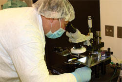
Workers in the clean room are required to wear a protective suit of gloves, a coat, a hairnet, shoe covers and a mask to ensure that the clean environment is not compromised, and that no harmful chemicals touch their skin, Kolesar said.
“The quality of air and the cleanliness of the facility are cleaner than a surgical suite,” Kolesar said.
Air in the clean room is purified and recirculated 13 times each hour to flush out any bacteria or dust in the room because any particle can damage the wafer, Kolesar said.
The clean room contains a high-resolution monitor connected to a video camera, which is used instead of a microscope to see the circuits being created, Kolesar said. He said circuits are created using photolithography, a process that uses ultraviolet light projected through a shaped mask to form a pattern on the aligned wafer.
Six different layers, chosen because of their unique electrical function, are added to the wafer through a process involving photolithographing, chemical washing and drying and heating, Kolesar said.
The wafers in their final stage are tested using an electric probe station, which connects to the wafer with small probes to test the circuits for conductivity, Kolesar said.
Upon completion of the course, students will take their finished silicon wafer home as a mark of their achievement, Kolesar said.

